
Close your eyes and imagine the following scene. No. That won’t work, will it? Let’s try doing this a different way. Keep your eyes open and imagine they’re closed. Visualize a future timeline where you use a GUI to drag-and-drop chiplets onto an active silicon substrate, run simulations and profiling, fine-tune your design, pick a package type, assign package pins, press the “Go” button, then sit back and wait for your new masterpiece to arrive back from the foundry. Well, we’re one step closer to such a future.
Before we plunge headfirst into the fray with gusto and abandon, please indulge me while we first take a few moments to set the scene and ensure we’re all tap-dancing to the same skirl of the bagpipes.
I love the smell of fresh silicon in the morning. Silicon chips are great, and they’re getting greater all the time. When I designed my first ASIC in 1980, it was at the 5-micron (µm) node and contained only around 300 equivalent logic gates, which equates to around 1,200 transistors. Admittedly, that’s not many transistors, but I used and abused every one of the little scamps, and by golly I made them sing like they’d never sung before.
Over the years, the size of the physical structures we could create on silicon chips got smaller and smaller. I remember the heady days when we were introduced to the 3µm node in 1982-83, 2µm in 1984-85, 1.5µm in 1986-87, and 1µm in 1988-89. I also remember the naysayers proclaiming that we’d never get below 1µm, and they kept saying “thus far, but no farther” every time we broke through a new barrier, with 0.8µm in 1991-92 and 0.6µm in 1993-94. 0.35µm in 1995, and… you get the idea.
Now, in 2026, mass production and commercial manufacturing are already underway at the 2-nanometer (nm) node, marking the transition from FinFET to Gate-All-Around (GAA) nanosheet transistors. Almost unbelievably, people are talking about devices at the 1nm node coming online by 2030 (we’re anticipating 1.6nm, 1.4nm, and 1.2nm intermediate sub-nodes along the way).
And if you think all of this is straining the bounds of possibility (and/or the bounds of credibility), it looks like we’re about to enter sub-nanometer space (where no one can hear you scream). For example, IBM Research is already experimenting with the world’s first 0.7nm chip technology.
Now, remembering that a micrometer (micron, µm) is 10-6m and a nanometer (nm) is 10-9m, you might expect us to start transitioning to picometers (pm), where a picometer is 10-12m. This would make IBM’s 0.7nm process a 700pm process. Indeed, this may well be the way we go; on the other hand…
The Swedish physicist Anders Jonas Ångström (1814–1874) was a pioneer in spectroscopy (the study of light emitted or absorbed by matter). In 1868, he published a landmark atlas of the solar spectrum, measuring thousands of spectral lines. To express these tiny wavelengths conveniently, he used a unit equal to 10-10m. Although he didn’t initially name the unit after himself, other scientists soon began referring to this unit as the ångström (Å) in his honor.
For more than a century afterward, the ångström became the standard unit for atomic dimensions, crystal lattice spacings, chemical bond lengths, X-ray crystallography, and the wavelengths of visible light.
Sad to relate, the ångström is not an official SI unit, even though it’s exactly defined as 1Å = 10-10m = 0.1nm. When the International System of Units (SI) became dominant in the 1960s and 1970s, scientists were encouraged to use SI prefixes like micrometers, nanometers, and picometers instead of non-SI units such as the ångström. However, practitioners in some domains, such as chemistry and crystallography, still frequently use Å as their unit of choice.
In 2021, Intel unveiled its new process roadmap under CEO Pat Gelsinger. At the same time, the company announced a wholesale renaming of its process technologies: the 10nm Enhanced SuperFin process was to be called Intel 7, its 7nm process would be known as Intel 4, and its next-generation EUV process would be known as Intel 3.
Now, this is the interesting bit, because its 2.0nm class would be known as Intel 20A, and its 1.8nm class would be known as Intel 18A. They chose to use the plain letter A rather than Å because it avoids keyboard and font issues, and it allows the nodes to be pronounced “Twenty A” and “Eighteen A,” for which we can all be truly grateful.
When Intel introduced this convention, it explicitly described the 20A node as “Ushering in the Angstrom Era.” Personally, I would be more than happy to refer to IBM’s 0.7nm (700pm) process as the 7A node. Intel may have started the trend, but TSMC has now joined the party with its A16 (1.6nm) and A14 (1.4nm) nodes, which it describes as “angstrom-class technologies.” It seems that the “Angstrom Era” is no longer just a marketing slogan—it may well become the industry’s next chapter.
But wait, there’s more! As if all this weren’t confusing enough, the numbers in the node names no longer correspond to the physical size of structures in or on the silicon. Back in the early days, a process node roughly described the size of key transistor dimensions—such as gate length—or interconnect features. By the time we reached around the 90nm generation, that relationship was beginning to unravel. Today, if we’re being charitable, we might say that names like 5nm, 3nm, and 2nm are best thought of as generation labels rather than ruler measurements. Alternatively, if we were feeling less charitable, we might be moved to mutter ungentlemanly things about marketing weenies sticking their fingers where they don’t belong, but we digress…
The point of all the above (yes, of course there’s a point) is that today’s high-end silicon chips can pack tens of billions of transistors onto a single die, but we are pushing up against the reticle limit—the maximum die size that can be printed in a single lithography exposure.
One solution is to abandon the idea of creating a single humongous monolithic chip (die). Instead, the design can be partitioned across several smaller chiplets, which are then connected and packaged to form a multi-die system.
As we’ve discussed before, companies such as AMD, Intel, and Nvidia have been doing this for quite some time. In some cases, this involves implementing high-speed I/O functions—such as SerDes—on proven, lower-cost chiplets, while the main digital logic chiplet is fabricated using the latest and greatest process node. In other cases, such as Nvidia’s GPUs, it involves connecting multiple reticle-sized compute dies (mega-chiplets, if you will) with stacks of high-bandwidth memory (HBM).
The thing is that none of this is easy. The reason companies like AMD, Intel, and Nvidia can do it is that they control the entire hardware and packaging ecosystem. To make chiplet-based design practical for everyone else, we’re now seeing groups of like-minded companies collaborating to develop common chiplet interfaces, packaging technologies, and interoperability standards.
The dream is that, one day, designers will be able to buy off-the-shelf chiplets from multiple vendors, combine them with any custom chiplets they choose to develop themselves, and stitch everything together to create a complete multi-die system.
We aren’t there yet, but we may be one step closer. All of the above brings us to a conversation I just had with Andreas Olofsson, who is the CEO of Zero ASIC. We’ve met Andreas before (see Is This the Future of Chiplet-Based Design?).
Most multi-die systems employ a passive silicon substrate whose primary job is to carry signals between chiplets. By comparison, the folks at Zero ASIC have developed a concept involving a suite of standardized chiplets mounted on an active silicon substrate that contains a built-in Network-on-Chip (NoC), along with the buffers, registers, and other infrastructure required to move data between the chiplets.
In fact, calling Zero ASIC’s implementation a substrate almost undersells the concept. Andreas often refers to it as “a chip in its own right,” noting during our conversation, “We have four billion transistors on our substrate” (all I can say is “Wow!”).
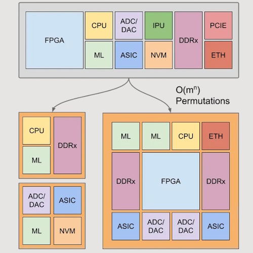
The image below provides a high-level visualization of how chiplets from a standard library can be combined in different ways to create a variety of multi-die systems. Note especially the FPGA chiplet. This employs Zero ASIC’s Platypus eFPGA technology, which can be thought of as the FPGA equivalent of RISC-V. Just as RISC-V provides an open instruction set architecture (ISA) that anyone can implement, Platypus provides an open eFPGA architecture that can be fabricated by different foundries using different process nodes. The goal is to free designers from proprietary FPGA fabrics and make configurable logic just another reusable building block in the chiplet ecosystem.
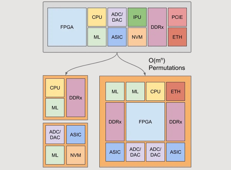
A suite of standardized chiplets (top) can be composed into multiple designs (bottom) (Source: Zero ASIC)
Since we last spoke, Zero ASIC has taped out and received its first prototype silicon, including its active fabric, a Platypus FPGA chiplet, and a quad-core RISC-V CPU test chip. These are engineering vehicles rather than production devices, but they demonstrate that the underlying concepts have made the leap from architectural vision to working silicon.
However, the reason Andreas called me wasn’t to tell me they’d received their first silicon. It was to tell me they’d removed what may prove to be another important obstacle on the road toward fully automated chiplet-based design. Up until now, Zero ASIC’s software could automatically place chiplets onto the active substrate, generate the network-on-chip connections between them, and produce any required FPGA configuration data. From there, however, the design still had to pass through the largely manual world of package layout. That’s the bottleneck they have now set out to eliminate.
In today’s flow, package design often involves handing a spreadsheet to an OSAT, waiting for engineers to create the package layout, reviewing the results, requesting changes, and repeating the cycle until everyone is happy. It’s a labor-intensive process that doesn’t sit comfortably beside the “press Go” philosophy driving the rest of Zero ASIC’s design flow.
To address this, Zero ASIC has developed what it calls a package compiler. Given a completed chiplet design and a target package style, the software automatically generates a design-rule-clean package layout, routing the connections from the chip bumps to the external BGA (or other package) pins. Today, the resulting package can be verified using existing third-party signal-integrity tools; over time, Andreas expects more of that verification to become integrated into the flow.
Viewed in isolation, an automated package compiler might not sound especially exciting. Seen as part of Zero ASIC’s broader vision, however, it’s another important step toward a future in which designing a custom chip becomes little more than selecting the required chiplets, pressing “Compile,” and waiting for the finished device to arrive in the mail.
Zero ASIC isn’t pretending the journey is complete. Although prototype chiplets now exist, the company still needs to expand its library before the concept becomes broadly useful. Andreas estimates that around $25 million of additional investment will be needed to build the minimum viable library—including essentials such as a DDR controller—required for widespread commercial adoption.
Whether Zero ASIC ultimately becomes the company that democratizes custom silicon design remains to be seen. But Andreas has spent the better part of fifteen years pursuing essentially the same vision—from the days of Adapteva, through Parallella, to today’s active-substrate chiplet architecture. Each step has moved a little closer to the same destination: making custom silicon something ordinary engineering teams can create without needing an army of specialists. That’s an ambitious—dare I say audacious?—goal. But if Zero ASIC succeeds, it could fundamentally change who gets to design custom silicon.
0 Comments
Log in to join the conversation.No comments yet. Be the first to share your thoughts.